Recently I have the need for the ability to log measurement into a digital format. Something that my Tektronix DMM cannot fulfill. With more than a dozen of HC908 MCU in my collection, and with some home made evaluation board available, I went ahead and utilize the eval board into action. The desired host PC interface, for simplicity, will be USB/RS-232 interface and this in turn requires the MCU to interface with a MAX-232-based board that I also have built in the past and lying around. The prototype or proof-of-concept nature of this project leads me to believe that the best way to do this is to cobble up together the boards, and just wire them ‘dead bug’ style when external components are needed.
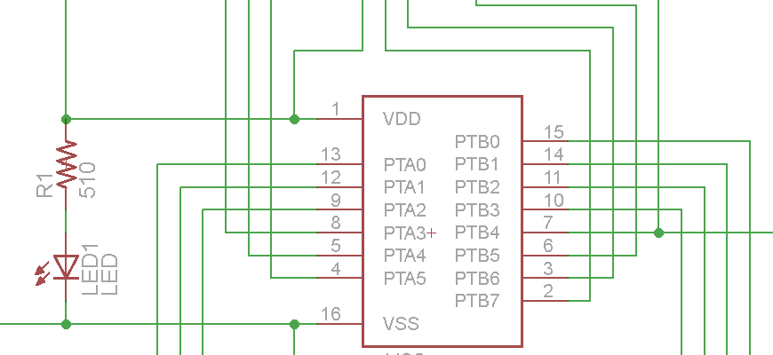
The idea is to use the ADC input of the MCU and use the computer to log the measurement results. The device that I have in mind itself is a rechargeable battery computerized tester. I quickly decide to use ADC channel 0 of the MCU, and some PORTB outputs for digital control. The only drawback is the fact that all ADC channels are in PORTA, and on MC68HC908QB8 MCU, some or all PORTA pins are used for the MON08 debug interface. It is necessary to unplug the ADC input from the circuit when doing debugging on the MCU.
Initial Setup, Noise
The initial setup of the system, for simplicity, uses no interrupt for the ADC reading. The ADC is setup in continuous conversion mode, and the software pulls the data periodically and send the result to the PC via RS-232. Sounds simple enough. However, the first readings of some measurement tests (a NiMH battery approx 1.2V in voltage) show that the value varies by as much as 40 milivolts. This initial setup, while serves the simplicity and expediency purposes, will become unwieldy if we demand accurate and stable measurements, something that I hope will compete with my Tektronix Tek DMM157.

void readmode(void)
{
     PTB |= 0xC0; /* turn on PTB7+6 */
     ADICLK = 0x16; /* 10-bit sw trig, long conv mode */
     ADSCR = 0x20; /* start continuous conversion of AD0 */
     mytog = 1;
     do {
          delay(1);
          lpctr = ADR; /* get the result, and the ADC will start another conversion */
          /* send the read result to host PC */
          esci_tx_lpctr(); /* the problem here is that when ADC is doing conversion
          after the above read, ESCI is blasting away creating extra noise */
          copybuf("\r\n");
          esci_tx_a();
          ...
          ...
The ADC itself is a 10-bit ADC (provides 1024 discrete values). With an approx. 5V reference voltage, this means that each count is approximately 5 mV:
(5V / 1024) = 5 mV
That is the smallest value that the system can read (resolution). I can give a little slack for quantization error, but it is 5 mv. 40 mV seems to be caused by external disturbances (my feeling).
The subject of ADC measurement itself is a very interesting subject with almost a dedicated science and professionalism in it. So, to support my objectives, I went ahead and do some more readings.
ADC Noise Elimination
Quick reading of the MCU manual reveals several things recommended by the manufacturer, Freescale. On top in my list is the inclusion of some capacitors to reduce circuit noise. The MCU environment is a very noisy digital environment and added into it is the connection to the host PC via USB/RS-232 adapter.
The manual states that VDD and VSS need to have a small ESR capacitor, and if exists, the Vref for the ADC. Vref pins are not available externally so I just put a ceramic 0.1 uF capacitor right across the VDD and VSS supply pins directly beneath the MCU. Another capacitor is needed at the ADC input channel, so the same capacitor is used, but I decided to place this directly on the measurement target (the NiMH battery input).

void readmode(void)
{
     PTB |= 0xC0; /* turn on PTB7+6 */
     ADICLK = 0x16; /* 10-bit sw trig, long conv mode */
     ADSCR = 0x00; /* start single conversion of AD0 */
     delay(1); /* MCU is busy waiting only, not doing anything else */
     __asm
          mov *_ADRH, *_adacc
          mov *_ADRL, *(_adacc + 1)
     __endasm;
     ...
     ...
Reading the manual and pondering it a bit gives me the impression that the writers suggests that the digital environment needs to quiet down a little when the ADC measurement is made. So this led me to think, that the MCU should not to anything (or reduce the tasks performed) when ADC conversion is happening. This led me to change the software. The MCU needs to just wait in a delay while conversion is on-going (shown in the code above). The RS-232 communication will have to wait until the conversion is done.
The above steps further reduce the variation of the measurement. My inital readings show that the fluctuations are now reduced to within 20 millivolts. So the actions that have been taken now has lead to a better measurement platform.
HC908QB8 as a Stable Measurement Platform
The steps above has shown me that external noise plays the majority of perturbation in the measurement result. I have decided to follow the recommendation made in the manual that the CPU be put into some ‘sleep’ mode to really quiet down the environment. The manual also suggests to perform averaging to get a more accurate reading.
The next step I took is enabling interrupt when ADC conversion is complete. This allows me to put a ‘wait’ instruction in the main code. This ‘wait’ instruction will shutdown some bus clocks, further reducing the system noise. The interrupt vector itself is an interesting find. Because I am using SDCC as a compiler, a kludge is employed to make the code looks nice (the interrupt list value is added by 1 to make it conform to the original Motorola interrupt list). See below:
/* all blank functions will point to the last non-empty function (rti) */
void adc_isr(void) __interrupt(15 + 1) __naked
{
     __asm
          mov *_ADRH, *_adacc
          mov *_ADRL, *(_adacc + 1)
          rti
     __endasm;
}
void kbd_isr(void)    __interrupt(14 + 1) __naked {}
void spitx_isr(void)  __interrupt(13 + 1) __naked {}
void spirx_isr(void)  __interrupt(12 + 1) __naked {}
void escitx_isr(void) __interrupt(11 + 1) __naked {}
void escirx_isr(void) __interrupt(10 + 1) __naked {}
void escier_isr(void) __interrupt(9 + 1) __naked {}
void tim1c3_isr(void) __interrupt(7 + 1) __naked {}
void tim1c2_isr(void) __interrupt(6 + 1) __naked {}
void tim1ov_isr(void) __interrupt(5 + 1) __naked {}
void tim1c1_isr(void) __interrupt(4 + 1) __naked {}
void tim1c0_isr(void) __interrupt(3 + 1) __naked {}
void irq_isr(void)    __interrupt(1 + 1) __naked {}
/* just do rti */
void swi_isr(void)    __interrupt(0 + 1) __naked
{
     __asm
          rti
     __endasm;
}
...
...
void readadc(void)
{
     adcnt = 0;
     lpctr = 0;
     do {
          /* the following method is a very stable ADC reading platform as
          recommended in Freescale document */
          ADICLK = 0x97; /* 10-bit sw trig, long conv mode */
          ADSCR = 0x40; /* start single conversion of AD0, generate interrupt
                           when done */
          __asm
               wait
          __endasm;

          lpctr += adacc;
          adcnt += 1;
     } while (adcnt != 16);
     lpctr = lpctr / 16;
     /* doing an average of 16 readings provides a very accurate ADC result */
}
The result? A great further stabilization of the measurement result. The reading now stays within 1 or 2 counts of variation (5 to 10 mV). Putting the contraption against my Tektronix DMM basically show that the measurement itself varies (the DMM says almost the same thing). So, I think the platform now is really stable with minimum noise being picked up.
The final step is to perform averaging. I didn’t want to resort to this method as this is pretty useless if your hardware itself, your platform, is still buggy. The optimum setup is if you have optimal hardware, then supported by optimal software. Both must be good to get the best result.
Averaging is done by taking 16 readings and accumulating (adding) them into a 16-bit value. Since the ADC itself is 10-bit, there are still some bits available for accumulation. Dividing by 16 is an easy process of shifting the accumulator right 4 times (ROR). It is important to note, that the accurate accounting of Vref is essential in achieving accurate measurement resut. In this setup, a python program in the host PC is responsible for converting the measurement result into voltage. The Vref value used is 4.99 Volt (not 5.0 Volt), as the output of a 7805 voltage regulator.
Conclusion
The final result of the above endeavor is a contraption that is comparable to my trusted Tektronix DMM. While readings may differ by 5 mV, I am guessing that it is quantization error and while I haven’t looked at the Tek spec, I am guessing it too has quantization error. I am very satisfied with the end result, the HC908 MCU is now tracking closely the DMM reading. The next challenge is probably to increase the resolution down to sub-5-millivolt level. There are some ideas brewing (voltage divider and lower Vref) but for a quick capacity testing of rechargeable batteries, the 5 millivolt accuracy is plenty enough for me.
Thanks for reading.
(Ketut Wiadnyana, June 2015)

It’s amazing what you can do with a processor that has an A/D – it can replace things that would have been complicated products years ago. I see that you use a 68HC908 – handy since you can use c. I’m using a PIC (actually, PICAXE) because it is cheap ($3), with a direct RS232 interface, and still has a 10-bit A/D like your Motorola part. I have to use BASIC to program it, but that’s enough for quick breadboarding.
One thing you may want to look at is your power supply. It seems that you’re using a line-powered USB adapter, which I’ve found to be horribly noisy for some switching supplies meant as chargers. No amount of capacitive bypassing seems to help as much as getting a quiet supply (or in the case of audio, going to battery power). The $3 PICAXE gives me a stable A/D reading with a good power supply, no software filtering needed.
LikeLiked by 1 person
Hi Rodericks, thanks for your note.
The power supply I use is a linear regulated bench supply. It may not be visible from the photo. While the RS-232/USB adapter is powered by the PC, *there is* a direct connection of the PC ground to the platform. I was thinking in the same line of thought too. PC ground is usually full of all kinds of spikes. My thinking is that, for a super stable platform, I’d insert some optocouplers to isolate the platform from the USB adapter, therefore isolating the two grounds and I get to keep the supply from a linear regulated PSU and it is the best. But hey, maybe that’s for the next project.
The choice of HC908 was from old habit acquired at Ford Motor Company a while ago. “The CPU has a divide instruction and linear memory”, so they said. The C code may be a bit unwieldy, especially that I use SDCC (GNU) compiler. But hey, for quick experiment enthusiasts like you and I, I think anything that can be cobbled together quickly is the right tool for the job.
LikeLike